
Building Functional Computer Memory from Scratch in a Backyard Shed is Possible, Just Not Easy
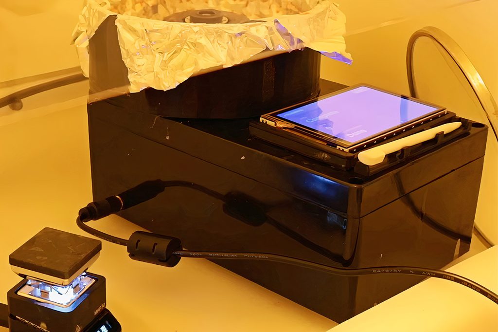

Dr. Semiconductor transformed an ordinary garden shed into a facility for the assembly of actual working memory chips. He had already set up the air filters and controls a few months before to maintain dust levels low enough to allow for careful operations.
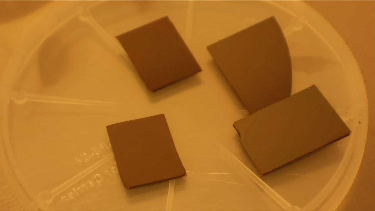
The materials needed began with silicon wafers, which served as the operation’s base. Each one was broken down into tiny pieces with highly exact cuts following natural crystal lines, just to prepare them ready for what was to come. The wafers were then cleaned with acetone and isopropanol to remove any surface imperfections that might cause problems later. Once they were thoroughly cleaned, they were placed in a furnace set to 1,100 degrees Celsius. An oxide layer began to grow on the surface and increased to a thickness of approximately 3,300 angstroms, since this insulating barrier serves as the foundation for all subsequent transistors and capacitors.

Crucial 32GB DDR5 RAM Kit (2x16GB), 5600MHz (or 5200MHz or 4800MHz) Laptop Memory 262-Pin SODIMM…
- Boosts System Performance: 32GB DDR5 RAM laptop memory kit (2x16GB) that operates at 5600MHz, 5200MHz, or 4800MHz to improve multitasking and system…
- Accelerated gaming performance: Every millisecond gained in fast-paced gameplay counts—power through heavy workloads and benefit from versatile…
- Optimized DDR5 compatibility: Best for 12th Gen Intel Core and AMD Ryzen 7000 Series processors — Intel XMP 3.0 and AMD EXPO also supported on the…
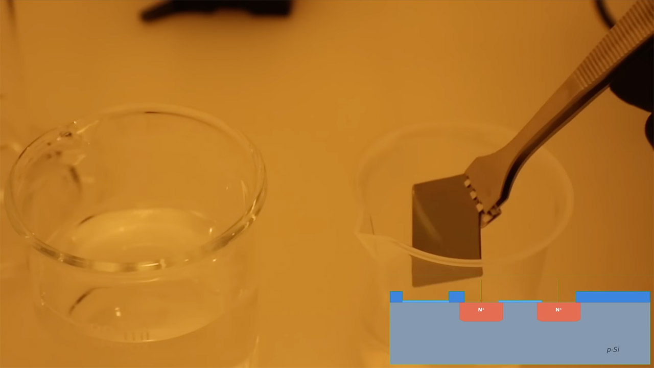
To begin creating the circuit layout, a slurry of photoresist and liftoff resist was spun evenly across the oxide. The appropriate pattern masks were then applied, allowing ultraviolet light to reveal the necessary locations. The photoresist that was exposed to UV light was then scraped away, revealing clear pathways to the silicon beneath, where the circuitry will be created. Then dry etching was used to cut out the paths all the way through the silicon.
The areas were then converted into conductors by doping them; all that was required was to lay a phosphorus-rich glass on top, then heat and anneal it at high temperatures, and all of the phosphorus atoms ended up in the silicon. This constructed the routes that each transistor need to function. Following that, a second round of resist coating and ultraviolet patterning specified the transistor gates and capacitor plates. This time, another oxide layer began to form in similar locations, but it was thinner, measuring around 20 nanometers, and the furnace temperature was slightly lower, at 950 degrees Celsius. This oxide layer was more limited in the amount of charge it could carry.
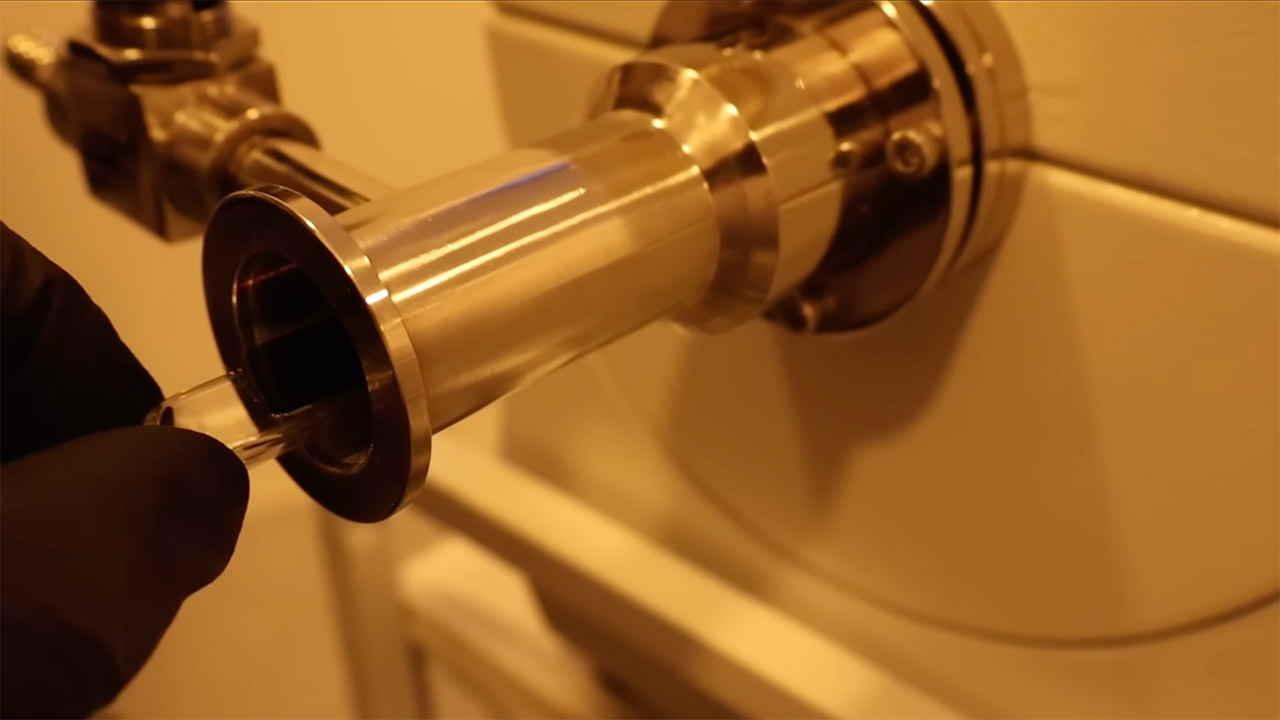
The next step was using hydrofluoric acid to create microscopic holes in the oxide where the metal would eventually be bonded. Next, a thin, uniform layer of metal was formed using a technique called sputtering. When the resist was removed with a solvent bath, the metal gates, contacts, and capacitor caps remained in their respective placements. That was it; the 5by4 array was built and placed on the wafer, with transistor gates smaller than a micron and each cell measuring a mere micrometer across.
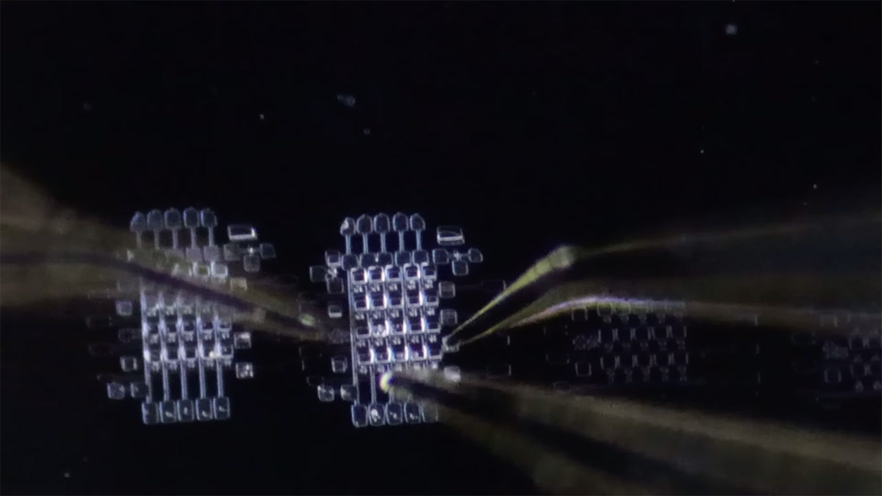
Probes made contact with the finished cells to begin the first tests, and when a small voltage was supplied to the gate, the transistor flashed on and off exactly as it should. A capacitor was charged to 3 volts and then held for around 2 milliseconds before slowly leaking away. The fact that it didn’t carry that charge for very long meant that the cells needed to be updated far more frequently than the memory inside a standard computer, but the basic principle worked perfectly. Data entered and exited through the transistor switch, just as it does with DRAM in principle.
[Source]
Building Functional Computer Memory from Scratch in a Backyard Shed is Possible, Just Not Easy
#Building #Functional #Computer #Memory #Scratch #Backyard #Shed #Easy